Applications of laser diode injection locking (1995 – 2000)
1. Introduction
The lasing wavelength of a laser diode can be locked to that of an injection
beam when the free-running lasing wavelength of the former is close to
the wavelength of the latter [1]. This phenomenon is known as injection
locking.
In this work, we proposed and demonstrated an optical signal inverter,
an optoelectronic chaotic system, and dynamic optical memory based on the
injection locking phenomenon.
2. Optical signal inverter[2]
Figure 1 shows a schematic illustration of the optical signal inverter,
which consists of two laser diodes, LD1 and LD2, with the same structure
but slightly different lasing wavelengths, a narrow-band etalon, and two
lenses. In addition, a beam splitter, two photo-detectors, PD1 and PD2,
and an oscilloscope are used to observe the temporal waveform of LD1, the
output power P1, and the inverted optical signal Po.
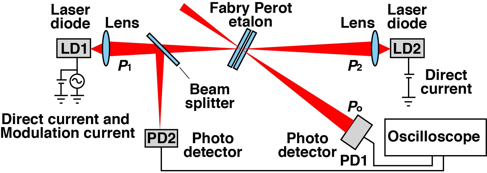
Fig. 1 Optical signal inverter proposed in this work.
Figure 2 shows the longitudinal modes of LD1 and LD2, the transmission spectrum of the narrow-band etalon, and the respective lasing wavelengths of LD1 and LD2. The laser diodes have equidistant longitudinal modes whose spacing depends on the cavity length and the effective refractive index. In general, the wavelengths of the longitudinal modes for LD1 and LD2 differ slightly due to the difference in the effective refractive indices, as shown in Fig. 2(a), and this wavelength difference, Δλ can be controlled by varying the temperature and injection current of the laser diodes. First, the wavelength of the longitudinal mode of LD1 is set to be slightly shorter than that of the longitudinal mode of LD2 by adjusting the temperature of the laser diodes. Under this condition, each laser diode usually lases with a single longitudinal mode, as shown in Fig. 2(c). Here λ1 and λ2 denote free-running lasing wavelengths of LD1 and LD2, respectively. Then, the transmission center wavelength, λC, of the narrow-band etalon is set to λ1 by tilting the etalon, as shown in Fig. 2(b). In this case, the output light of LD1 couples to LD2, while the output light of LD2 does not couple to LD1, because it is reflected at the etalon. As the injection current of LD1 is increased, λ1 also increases due to thermal effects, and Δλ accordingly decreases gradually. When |Δλ| becomes smaller than the injection locking width, the lasing wavelength of LD2 locks to that of LD1 as shown in Fig. 2(d). As the injection current of LD1 increases further, |Δλ| increases again. Then, the lasing wavelength of LD2 unlocks and returns to the free-running lasing wavelength λ2 when |Δλ| becomes larger than the injection locking width. Accordingly, one can obtain the inverted signal for the output power of LD1 by detecting the output power of LD2 reflected at the etalon using PD1.
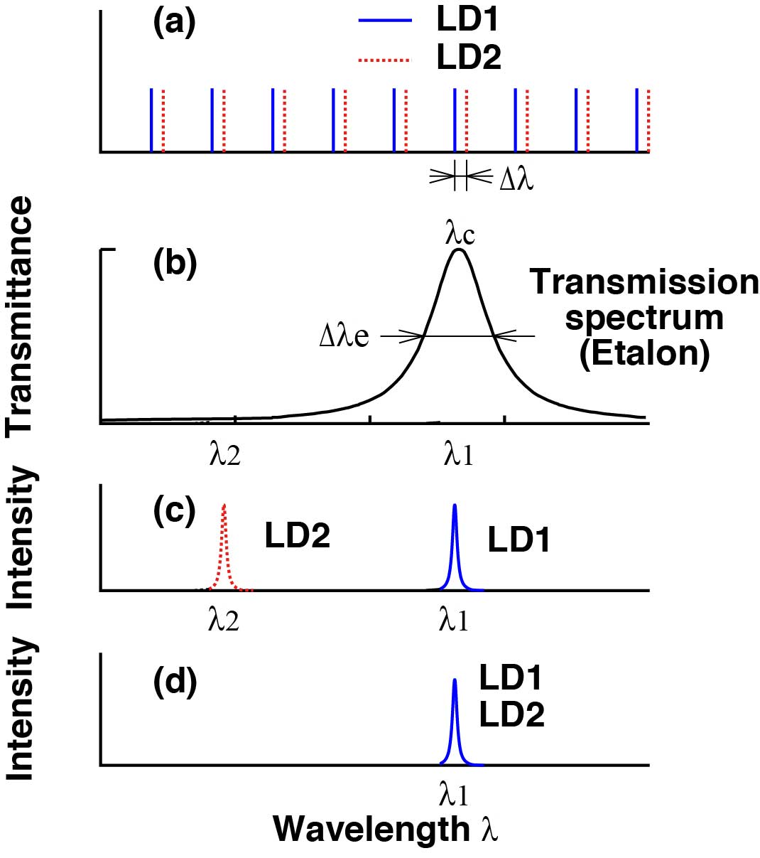
Fig. 2 (a) Longitudinal modes of LD1 and LD2, (b) transmission spectrum of the etalon, (c) lasing spectrum of LD1 and LD2 under free-running conditions, (d) lasing spectrum of LD1 and LD2 under injection locking conditions.
Figure 3(a) shows the experimental result of the injection locking phenomenon, which was obtained when the output power of LD1, P1, was set between 7 mW and 10 mW. As a result, a decrease in the power detected at PD1, Po, was observed. Figure 3(b) shows the temporal waveforms of P1 (blue line) and Po(red line) under direct current modulation of LD1. By adjusting the amplitude of the modulation current appropriately, an inverted optical signal for the LD1 output power was obtained.
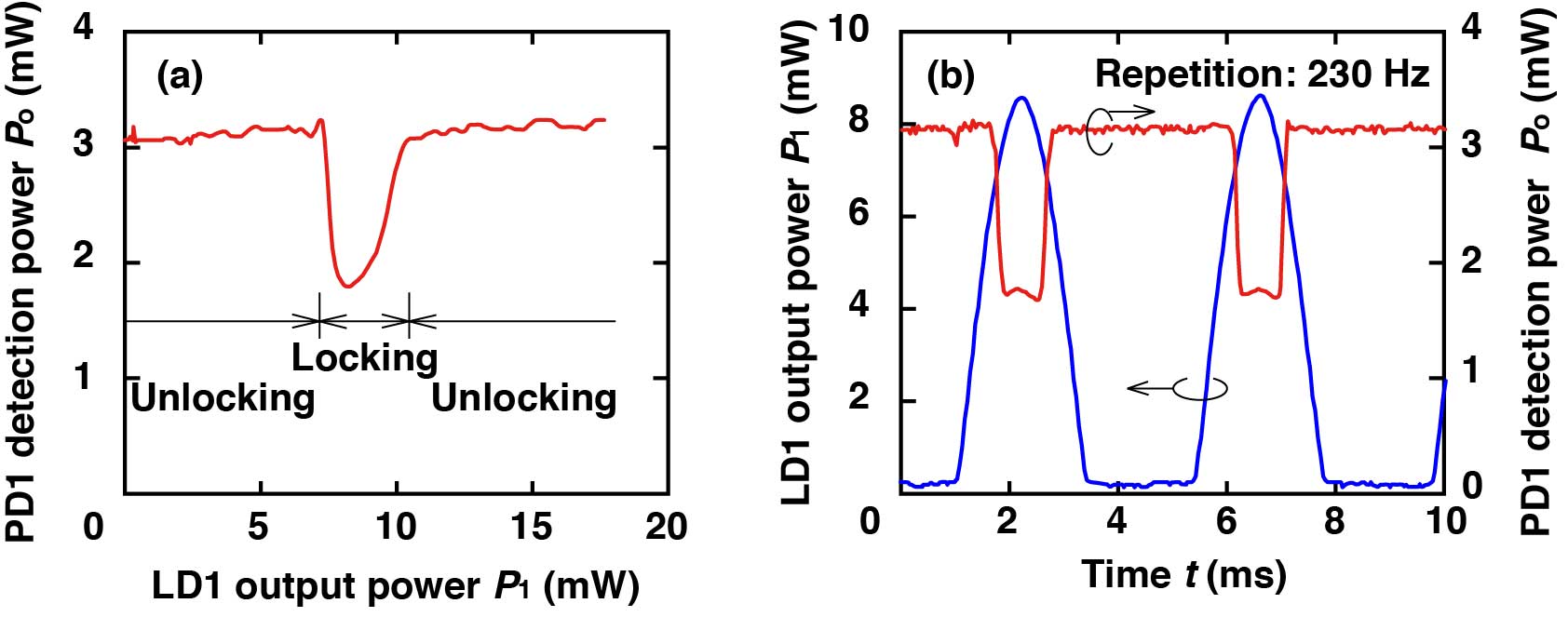
Fig. 3 (a) P1 vs.Po and (b) demonstration of the inverter operation (temporal waveforms of P1 and Po).
Although the optical signal inverter requires precise adjustment of the
optical components and operation parameters (e.g., temperature and injection
current of the laser diodes, transmission center wavelength of the etalon),
and despite the fact that the response time is restricted by thermal effects,
the operation principles of the signal inverter are interesting from the
viewpoint of fundamental laser physics.
3. Optoelectronic chaotic system [3]
Applications of laser chaos to optical dynamic memory and secure communication
were investigated extensively at the time of this research. One popular
approach for generating a chaotic signal is to add a delayed feedback loop
to a nonlinear system with adequate input-output characteristics. The input-output
characteristics shown in Fig. 3(a) are suitable for a chaotic system.
In this work, we proposed and demonstrated an optoelectronic chaotic system,
in which PD detection signal is delayed, amplified, and fed back to the
LD1 injection current, as shown in Fig. 4.
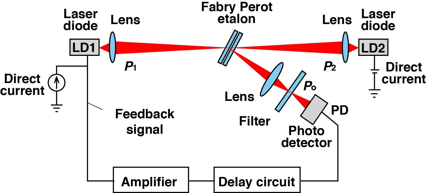
Fig. 4 Optoelectronic chaotic system.
Figure 5 shows the temporal waveforms of the power detected at PD, Po. As the feedback gain increases, the temporal waveform changes from the stable state shown in Fig. 4(a) to the period-two state, in which two alternating output levels appear, as shown in Fig. 4(b). Increasing the gain further, the waveform changes to the period-four state, in which four output levels appears periodically, as shown in Fig. 4(c), and then changes to the chaotic state, as shown in Fig. 4(d). We also reproduced the observed dynamics of the chaotic system using numerical calculations.
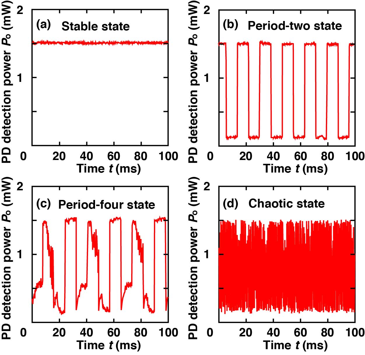
Fig. 5 Temporal waveforms of the measured power Po.
4. Dynamic optical memory [4]
The chaotic system shown in Fig. 4 exhibits a period-two state, in which
the output power exhibits alternating high and low levels with a period
corresponding to twice the delay time of the delay circuit. One can expect
that a non-return-to-zero digital optical signal injected to the chaotic
system during the time period of the low output power level will be inverted
repeatedly every round trip and stored in the chaotic system.
In this work, we studied the stability of the dynamic memory operation
using the period-two state. Figure 6 shows a schematic illustration of
the optical dynamic memory setup. We prepared an additional laser diode,
LD3, to inject a non-return-to-zero optical signal to the chaotic system.
Injection of the optical signal to PD was triggered by the falling edge
of Po. Then, the temporal waveform of Po was observed using an oscilloscope.
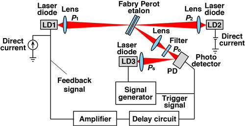
Fig. 6 Experimental setup of the dynamic optical memory operation.
Figure 7 shows one example of our experimental results. An 8-bit non-return-to-zero optical signal (01101100) was injected to the chaotic system. The signal was inverted repeatedly every round trip and stored in the system for a while. However, the stored signal was unstable and eventually disappeared. Our numerical simulation revealed that noise in the chaotic system causes the signal width to fluctuate and the stored signal to disappear.
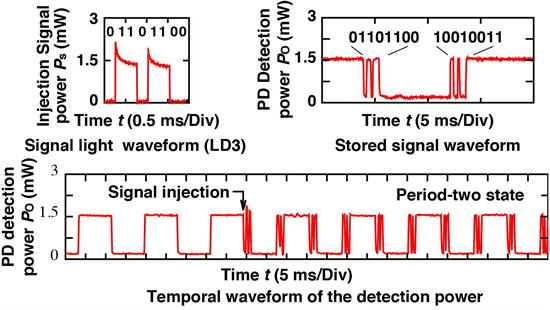
Fig. 7 Experimental result of the dynamic optical memory operation.
Acknowledgements
I would like to thank Matsushita Electric Industrial Co. Ltd. for providing
me with the laser diodes. This work was partially supported by the Electric
Technology Research Foundation of Chugoku.
References
[1] R. Ito and M. Nakamura, Semiconductor lasers, Baifukan, Tokyo, pp.
195-198, 1989 (in Japanese).
[2] T. Fukushima and T. Sakamoto, Optical signal inverter using injection
locking of coupled semiconductor lasers, Japanese Journal of Applied Physics,
vol. 36, part 2, no. 3A, pp. L280-282, 1997.
[3] T. Fukushima and T. Sakamoto, Chaos in coupled semiconductor lasers
with an electronic delayed feedback caused by injection locking, IEEE Journal
of Quantum Electonics, vol. 34, no. 5, pp. 750-758, 1998.
[4] T. Fukushima, T. Tanaka, and T. Sakamoto, Stability of optical dynamic
memory operation under period-two state of chaotic system, Japanese Journal
of Applied Physics, vol. 39, part1, no. 1, pp. 114-119, 2000.